ECE 1388: Final Project Report
16Kbit Content Addressable Memory
Mehdi Khanpour
Alexander Tomkins
Submitted: December 20, 2006
Abstract
The report describes the final implementation of a 16kbit Content
Addressable Memory (CAM) array in 0.35 um CMOS, completed as part of the final
design project of ECE 1388. The project
was designed entirely with custom logic in a hierarchical manner, using
pitch-matched cells and abutting wire connections between adjacent cells. The design is core-limited, with the
floor-plan being dominated by the 16
Introduction and Background
Content addressable memory, also known as associative
memory, is a memory type used in high-speed searching applications. A
CAMs see use in a wide range of
applications, from translation lookaside buffers in
modern microprocessors, to network address translation tables in high-speed
data switches. The major attraction of a
General Overview
The
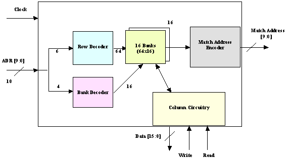
Figure 1: Top level block diagram.
Addresses are decoded between the 16 banks by the 4 MSBs through a 4-bit to 16 bank decoder, and the word-line is decoded via the 6 LSBs through a 6-bit to 64 word decoder. Through the column circuitry, read and write operations are enabled via external pad inputs and 16 data pads. When performing match operations, the search key is loaded on the data lines and, activated by the match-enable pin, a match signal will be generated on the appropriate word-line that is then encoded by the match address encoder to provide the location of the match.
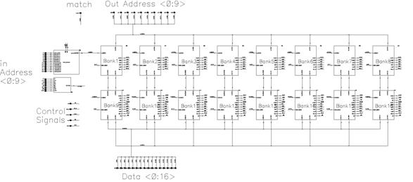
Figure 2: Final chip schematic.
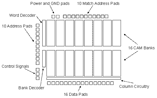
Figure 3: Final chip floor-plan.
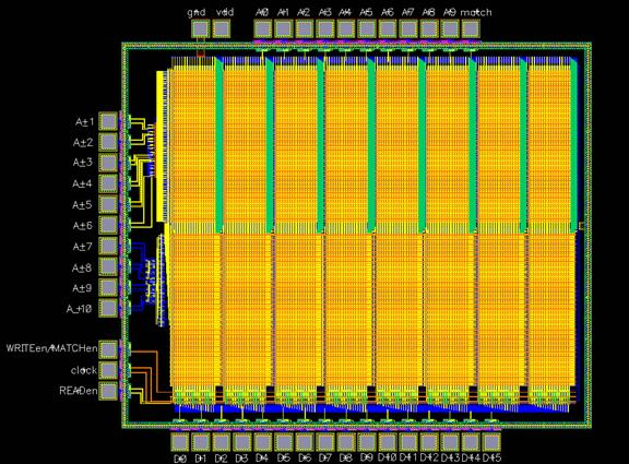
Figure 4: Final chip layout.
Figure 2 shows the final chip schematic, Figure 3 shows the final chip floor plan, and the final layout of the chip is shown in Figure 4. The chip dimensions are 2125umx1868um=3.97mm2 including the pad frame. The layout and circuit configuration of individual cell blocks can be found in the appropriate presentation material.
The final chip is DRC and LVS clean with the exception of warnings relating to minimum pad-pitch. These warning are related to wire-bonding requirements, and would be resolved should this design be fabricated. The LVS report is attached as Appendix 1.
Simulation Results
Simulations were carried out to demonstrate the functionality of read, write, and match operations. The simulations were done using a 10 ns clock period corresponding to a 100 MHz operation.
Figure 5 shows the transient simulation results for a sample read operation. The operation takes 1.5 clock cycles. During the high-lock, the bit and bit_bar lines are pre-charged. During the down-clock, the word-line is activated by the word-decoder, and either bit or bit-bar will get pulled down accordingly. During the next high-clock, the voltage difference is applied to the sense-amp which produces the output. On the second plot, the data-line can be seen to rise to match the cell content signal level.
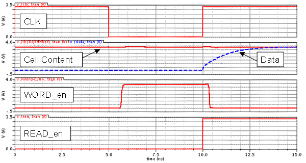
Figure 5: Transient simulation showing read operation.
Figure 6 shows the results of
a transient simulation of a sample write operation. During high-clock cycle, the bit and bit-bar
lines are pre-charged. During the
low-clock cycle the data is applied to the bit and bit-bar lines and the
word-line is raised by the word-decoder allowing the data to be written to the
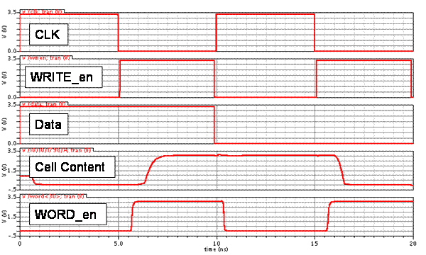
Figure 6: Transient simulation showing write operation.
Figure 7 shows the transient simulation results of a match operation being performed. The match operation is performed in one clock cycle. In the high-clock, the match-line is pre-charged high. During the low-clock, the data is put on the bit and bit-bar lines and compared to the cell contents. The following plot shows two successive match operations, matching the cell value, a logic ‘0’, against logic ‘1’ and then a logic ‘0’. On the fourth plot, the result of the match operation can be seen, first a mismatch, followed by a match signal.
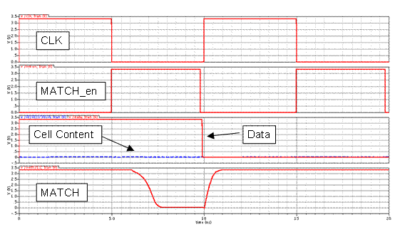
Figure 7: Transient simulation showing match operation.
Conclusion
The 16kbit